
A Miniaturized Discrete MC1466
September 28, 2014 Cleverness, Projects 15 CommentsUpdate: the bill of materials is now available. You can order boards from OSH Park using this direct link. Last time I ordered, it cost me a grand total of $3.55 for three boards (free shipping), and it took about two weeks for the boards to arrive.
I screwed up. My bench power supply is a Lambda LPT-7202-FM triple output (0-7V @ 5A, 0-20V @ 1.5A, 0-20V @ 1.5A), and I blew it up by trying to desulfate a lead-acid battery. The idea is to take a dead lead-acid battery and recondition it by charging it with a current-limited 15V source while feeding it high voltage pulses. I had a diode connected in between the battery and the bench supply to protect the power supply from the high voltage pulses. Well, the diode failed. It was a sad day.
Fortunately the service manual for the supply is available online. I traced around the circuit and found that two of the power control chips were fried, but everything else seemed OK–I could move the one remaining functional chip from channel to channel to confirm that. The control chips were marked with the Motorola logo and a Lambda house part number: FBT-031. A forum thread indicated that the part was actually the MC1466. Sadly this chip is long out of production and a bit hard to find, although a popular auction site had several listed from a seller in China (but who knows if the parts were counterfeit or not).
The datasheet has the full schematic including resistor values, but how do I know that it actually matches the chip? Since the IC is packaged in a ceramic DIP, I followed reader Uwe’s suggestion and took a chisel to one of the dead parts.
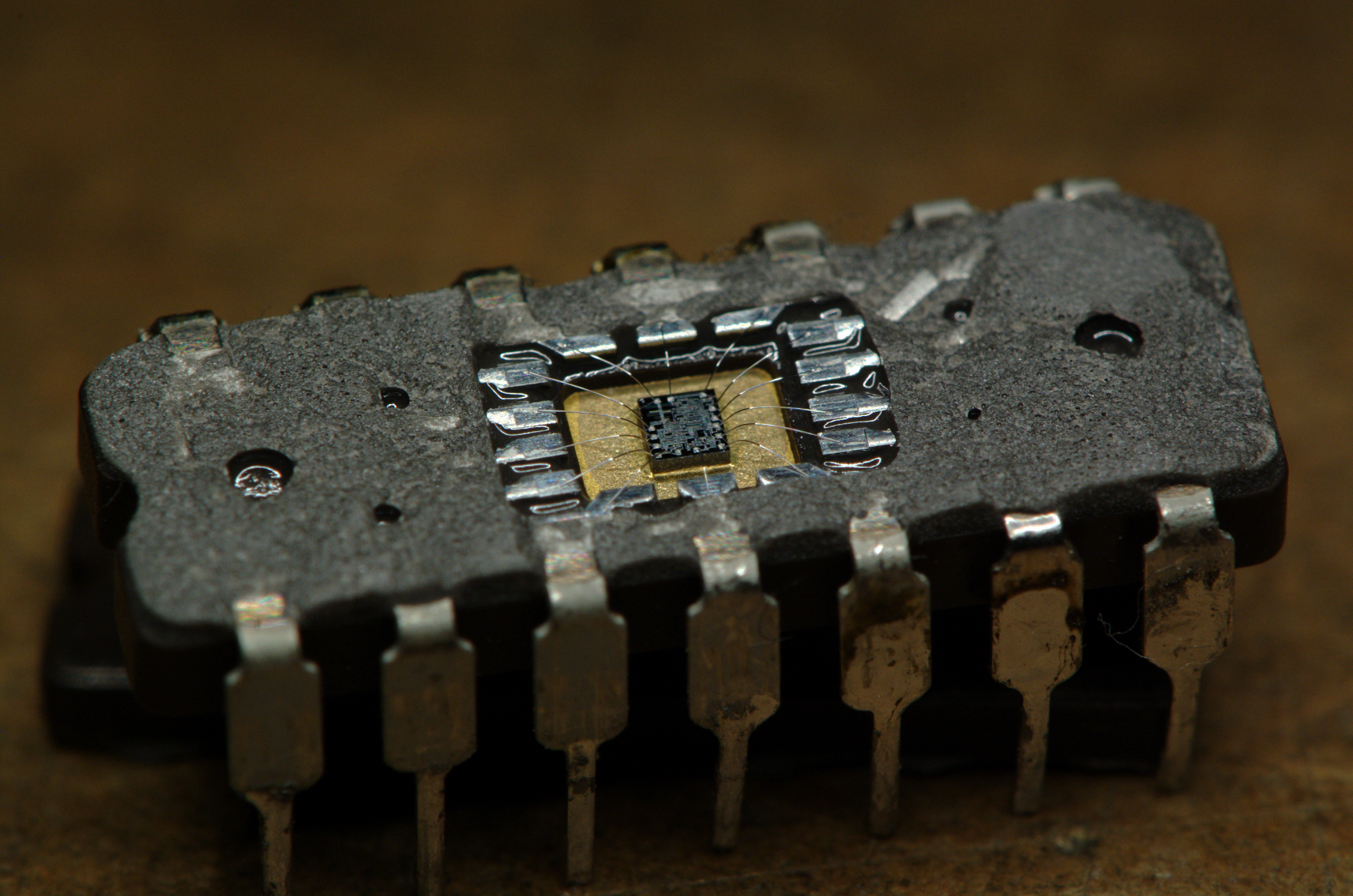
It worked and nothing was damaged! The die looks like this:

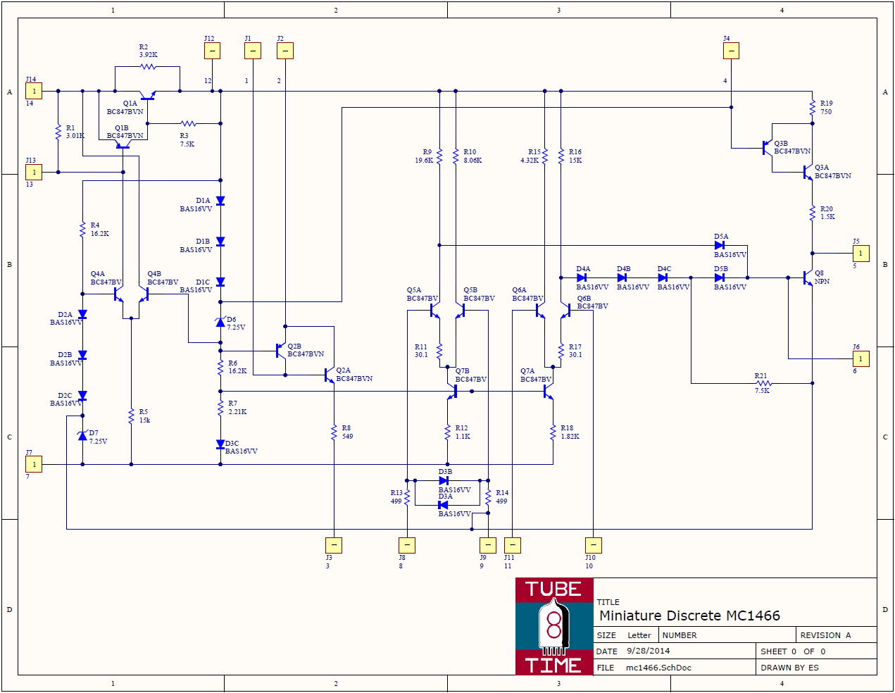
I went over the layout and it matches up with the datasheet schematic. Those funny round elements are actually zener diodes. You can see the long skinny resistors and the lateral PNPs as well as the NPN transistors and diodes. Below is the schematic (click to enlarge):
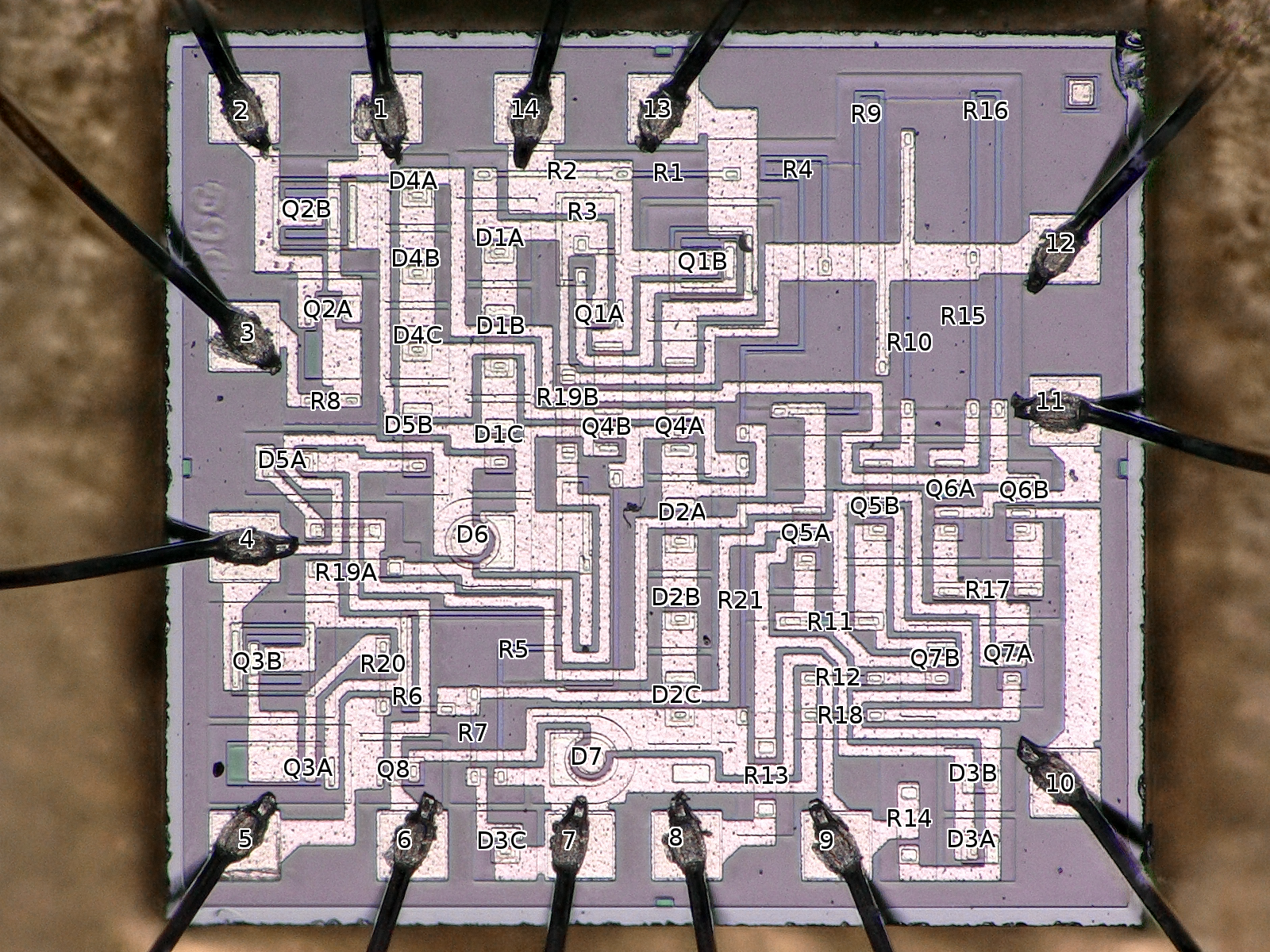
The IC design is pretty archaic. I’d say it dates to the late 1960s. There are fairly ordinary differential amplifiers, but the current mirrors are really strange, and the voltage reference circuit uses Zener diodes and series-connected diodes instead of a temperature compensated bandgap reference. The two Zener diodes (the only round features on the die) are probably just reverse biased NPN transistors, using the ~7.5V avalanche breakdown of the base-emitter junction. The lateral PNPs have a much higher breakdown voltage so they can’t be used this way.
Here’s a labeled die photo (click for a larger image) so you can see where each of the components are. The component designators match up with my schematic, not the IC datasheet schematic.
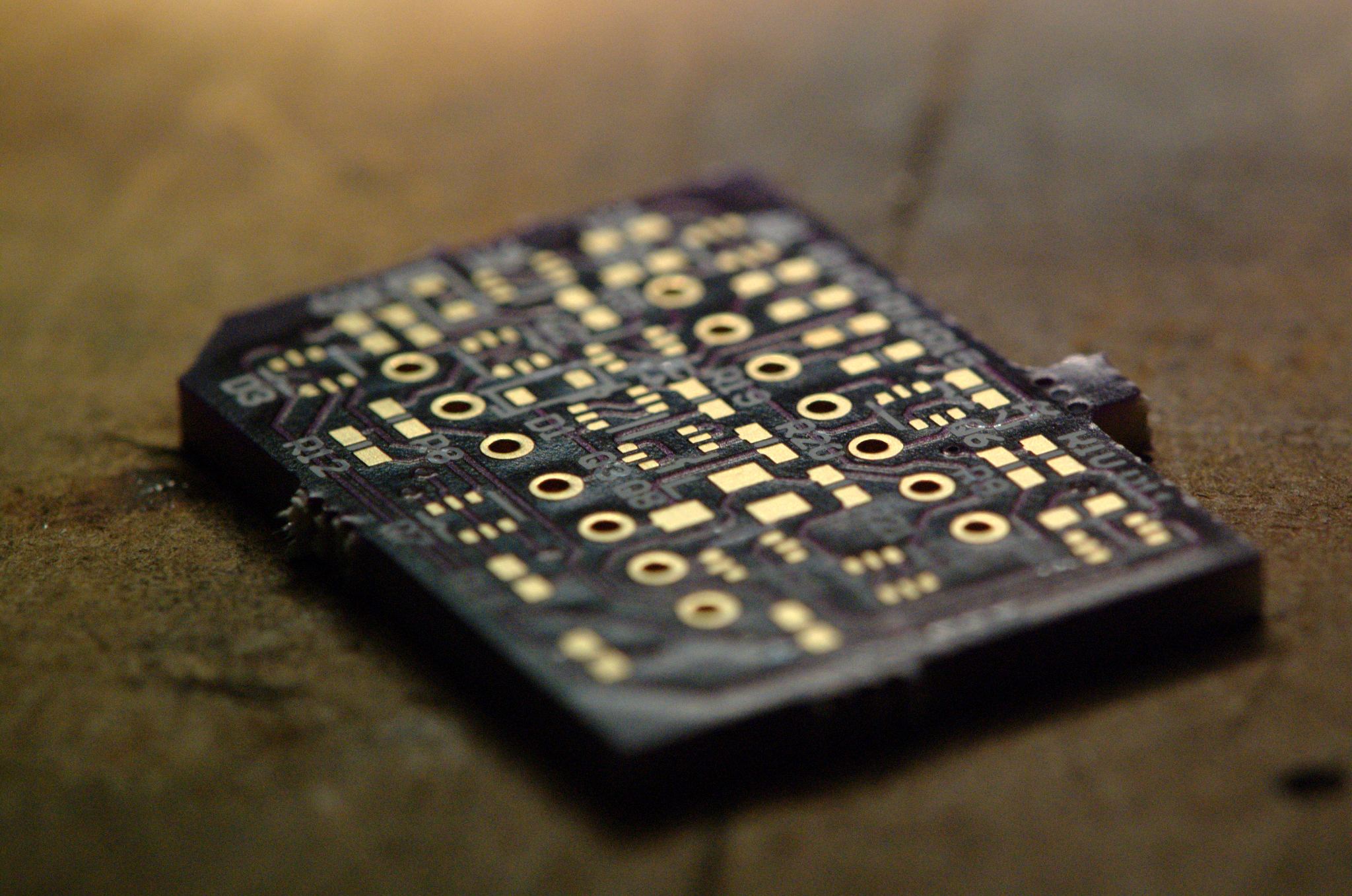
The device is simple enough that I decided to build a really small PC board with discrete components. I found that the BC847BVN (NPN/PNP dual transistor), BC847BV (dual NPN), and BAS16VV (triple diode) came in a really tiny SOT-563 package. Believe it or not, this is not the tightest or smallest layout I’ve done. This is a 2-layer board with 6 mil traces and 6 mil spaces.
To give you an idea just how small the SOT-563 is, take a look at the first BC847BVN I soldered:
![]()
The part is 1.05mm x 1.05mm! I had to use a very fine soldering iron tip and a microscope. Another trick is to use really thin solder (I used 0.38mm). As you can see, the resulting board is just slightly larger than the original DIP IC:
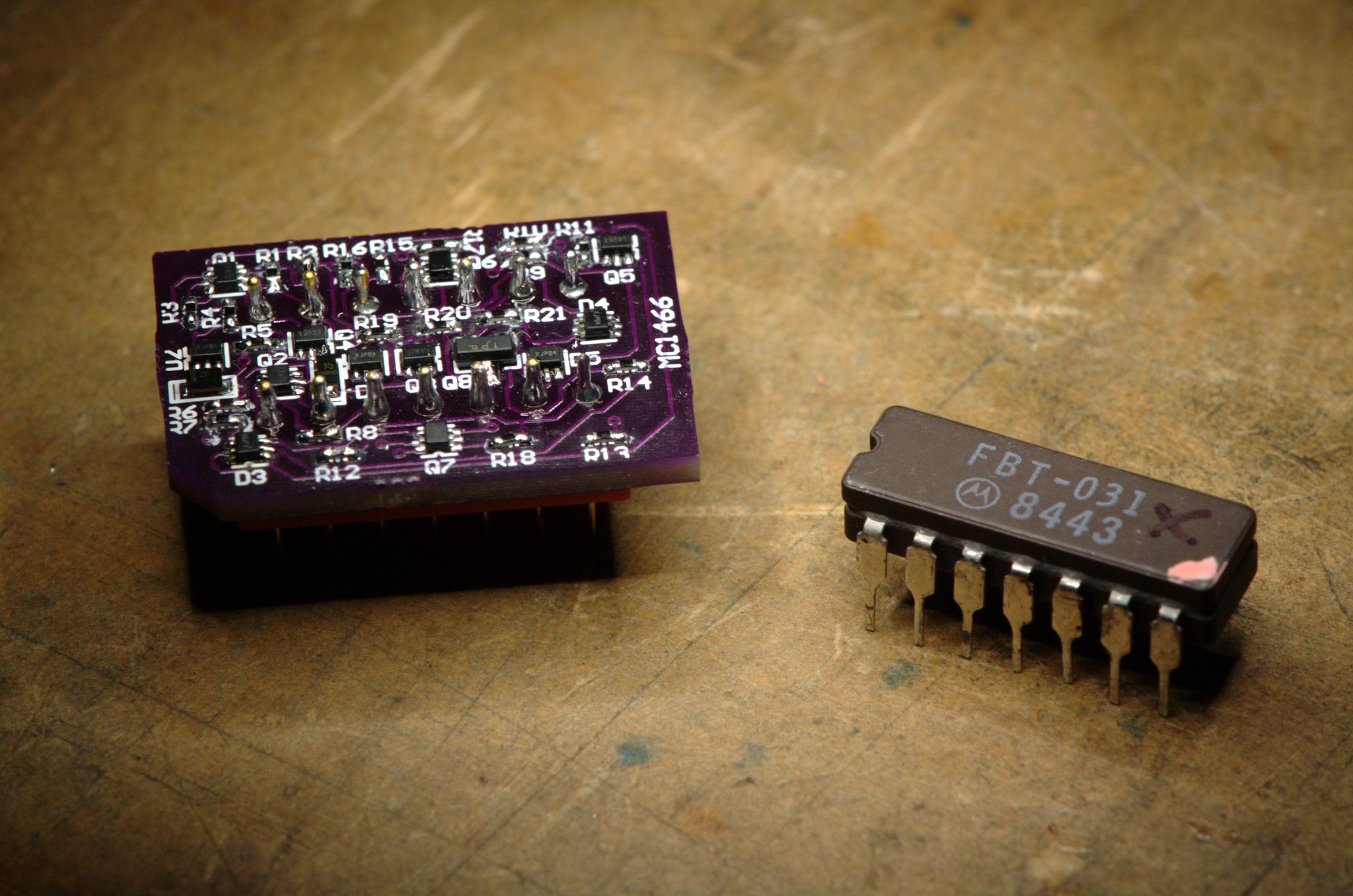
It really is pin compatible. I plugged two of them into my Lambda supply and now it works perfectly!


