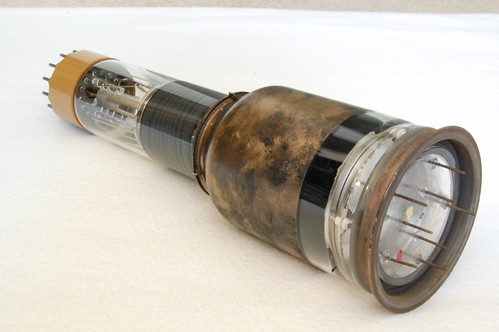
Sound Blaster 1.0 Principles of Operation

Cleverness No Comments

The Sound Blaster 1.0 was not the first PC sound card, but it was the first to support digital sound, two different types of sound synthesis, MIDI, and a joystick all in one card. Let’s lift the hood and examine how the card does its magic.
You can follow along by looking at the schematic here.

Sound Playback
There are three methods a Sound Blaster card uses to play back digital audio.

Direct DAC
The first is called Direct DAC and it means that the PC software has to feed the sound card each sample at just the right time. It works a lot like the parallel-port DACs that people used to build in the 80s and 90s, or like the Disney Sound Source. When you send a data byte to the sound card, it immediately changes the analog signal going into the speaker amplifier.

Software using this method typically sets up a periodic timer interrupt. In the interrupt handler, the new sample is calculated and then fed to the sound card for playback.

Although it’s a simple method, it produces extra noisy playback to due the timing jitter of the interrupt handler. Because PC interrupts are non-deterministic, the samples don’t occur at precisely the sampling rate. This timing difference means that the waveform being reproduced doesn’t match the source material, and the difference in voltage sounds like noise or hiss.

DMA DAC
The other method uses the DMA (Direct Memory Access) controller on the PC motherboard to automatically send samples to the sound card. It does require a little bit more work to set up the operation.

  1. The software configures the PC’s DMA controller (historically an Intel 8237) with the source address and length. The DMA controller is set to perform a single transfer per DMA request (DREQ).
  2. The Sound Blaster is configured for a particular sampling rate. It programs an internal timer to generate a DREQ signal at the sampling rate.
  3. The software sends the playback command to the Sound Blaster.

The next operations happen in a loop until all the samples have been played back. Notice that the software is not involved at all—just the DMA controller, the Sound Blaster, and main memory.

  1. The Sound Blaster asserts DREQ.
  2. The DMA controller responds by asserting DACK (DMA Acknowledge) at the same time it places the memory address and memory chip select onto the bus. The data byte gets transferred directly from main memory into the Sound Blaster input register!
  3. The Sound Blaster takes this data and sends it to the audio DAC.

Finally, the Sound Blaster ends playback then triggers an interrupt to let the software know that it is done with playback.

Auto-Initialize DMA DAC
The final method, introduced with the Sound Blaster 2.0, is very similar to the previous method, except the ending. The Sound Blaster triggers an interrupt as before, but then it reloads the sample counter to the original value and continues requesting samples from the DMA controller!

The usual way software uses this feature is to create a seamless digital audio stream using a double buffer. The DMA controller gets a buffer that is twice as big as the number of samples that the Sound Blaster is programmed to play back. Because of that, the interrupt gets triggered halfway through buffer playback. In the interrupt handler, the software then loads a new set of samples into the buffer half that has already been played. When playback hits the end of the DMA buffer, the interrupt triggers again, only this time the software refills the last half of the DMA buffer. The DMA controller then wraps around to the beginning of the buffer and playback continues unbroken.

One of the side effects of this approach is that if the software crashes, the DMA controller and sound card continue to play back the sample buffer in a loop. You may have heard this when playing old DOS games back in the day.

Sound Recording
This works in very much the same way as playback including the Direct mode, DMA mode, and Auto-Init DMA modes, except data gets transferred in the opposite direction, from the sound card into main memory.

One interesting wrinkle is that the Sound Blaster doesn’t actually have a proper ADC (analog-to-digital converter)! Instead it uses a clever circuit and an algorithm to accomplish the same thing:

  1. An input filter processes the incoming sound to smooth out any high frequency transients. This is common practice, even with an ADC, to help prevent sampling-induced aliasing, but it it’s helpful for making the trick work.
  2. A comparator looks at the difference between the audio DAC and the incoming signal. The output of the comparator is only one bit; it can only tell if the incoming signal is greater than or less than the setting of the audio DAC.
  3. The DSP starts the audio DAC at the halfway point, then looks at the comparator output. The comparator output gets recorded as the most significant bit of the audio sample.
  4. Depending on the bit, the DSP sets the audio DAC up or down half again—either 25% or 75%.
  5. The DSP repeats steps 3 and 4, going halfway again and again until it’s obtained the 8 bits of a complete sample.

This technique is known as successive approximation, and it’s a technique used in many ADC chips. The code looks something like this:

mov p1,#80h ; Start DAC at the halfway point, 1000 0000
mov c,t1 ; 1 Put comparator output into carry bit
mov p1.7,c ; 2 If greater, then leave MSB as is. If less, clear MSB
setb p1.6 ; 1 Set DAC to upper or lower halfway point
mov c,t1 ; 1 Check comparator output again
mov p1.6,c ; 2 Rinse and repeat
setb p1.5
mov c,t1
mov p1.5,c
setb p1.4
mov c,t1
mov p1.4,c
setb p1.3
mov c,t1
mov p1.3,c
setb p1.2
mov c,t1
mov p1.2,c
setb p1.1
mov c,t1
mov p1.1,c
setb p1.0
mov c,t1
mov p1.0,c
mov a,p1 ; We are done, copy DAC code into accumulator.

The Hardware, Section By Section

Address Decoder
The address decoder takes the I/O port address off the ISA bus and looks for accesses at 210h, 220h, 230h, 240h, 250h, or 260h depending on the jumper setting. It also looks for 388h and 389h so that it can make the Yamaha OPL2 chip appear there for Adlib compatibility. It also decodes 0x200-207h as the joystick port (each address is actually the same).

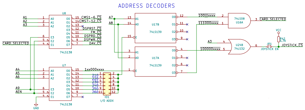
A jumper, JP1, can be pulled to shut off the PC joystick port. The MIDI function still works, however. Many combo-IO boards came with a built-in joystick port so the one on the Sound Blaster may not always be needed.

Reset Circuit
It’s important to make sure the card powers up in a good state without generating spurious noises, so the SB uses the ISA RESET signal to clear the OPL2, the CMS chips, the joystick one-shot, and basically all of the other internal state latches.

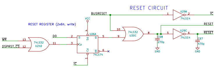
There is also an IO port that, if you write a 1 to it, resets the DSP and its associated bus interface. (You also have to write a 0 to it afterwards to allow the DSP to start operating.) Later versions of the DSP require this to exit high speed auto-init DMA mode, since in this mode, the DSP devotes 100% CPU to servicing DMA requests.

DSP
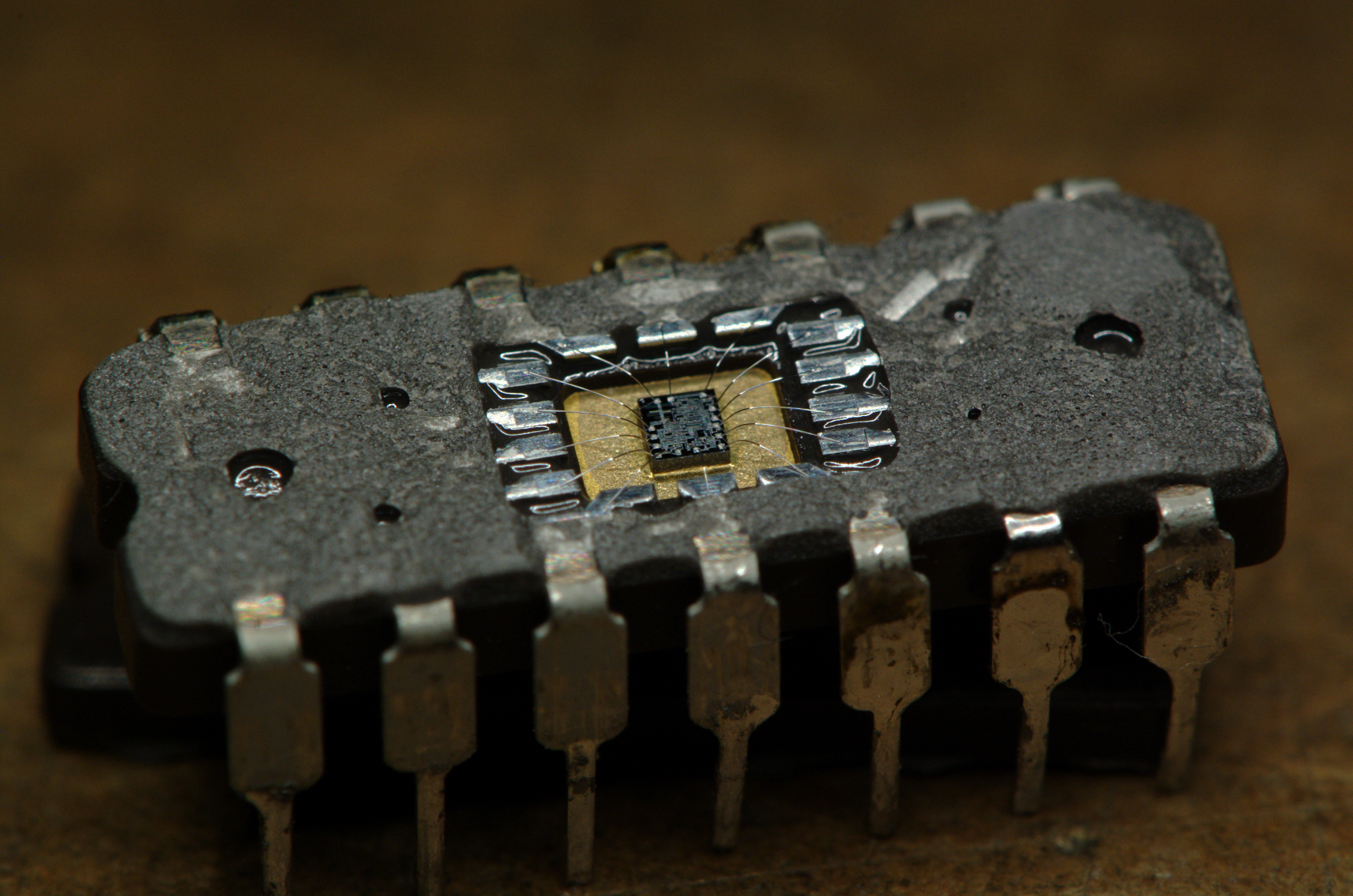
The core of the digital sound capabilities of the Sound Blaster is the Digital Sound Processor, or DSP for short. It’s not actually a Digital Signal Processor in the traditional sense—it’s just an 8051 microcontroller with custom firmware.

The DSP also handles MIDI transmit and receive using the 8051’s built-in UART.
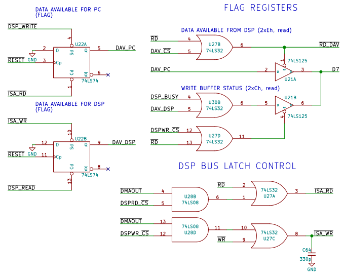
DSP Bus Interface
The bus interface allows the host PC to talk to the DSP. It uses two unidirectional 8-bit registers as a “mailbox,” temporary holding areas for a single data byte. One is for PC-to-DSP communications, and the other is for DSP-to-PC communications. There are also two data flip flops that are used to signal when data is available in one of the registers.

When the PC sends data to the DSP (I/O port 2XCh), the data gets stored in an 8-bit register and the flip-flop is automatically set high (DAV_DSP).

When the DSP reads the register, the flip-flop gets cleared automatically.

When the DSP sends data to the PC, the data goes into the other 8-bit register and the other flip-flop automatically gets set (DAV_PC). The PC can check this bit by reading from I/O port 2XEh. When it reads from I/O port 2XAh, it receives the byte of data and the flip-flop automatically gets cleared. The DSP can see that the PC has read the byte by checking the DAV_PC input. The DSP often checks this pin to make sure the PC has read a data byte before writing a new data byte to the register, otherwise the byte in the register will be lost before the PC has a chance to read it.
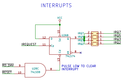
Interrupts
When the DSP is done with a particular (often lengthy) task, it can signal the host PC by asserting the interrupt line. It does this by pulsing IREQUEST which triggers a flip-flop that asserts the IRQ line on the PC bus. On the host PC, the interrupt handler is supposed to clear the interrupt by reading from I/O port 2XEh. This simply clears the flip-flop which then deasserts the IRQ line.
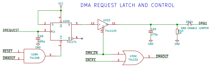
DMA
When the DSP needs a new sample from the PC (or needs to transfer a new sample to the PC during record mode), it pulses the DREQUEST line. Note that the DSP also needs to enable DMA by asserting its DMA_EN# line. When DREQUEST pulses, it causes the DMA request flip-flop to output a 1 on the DRQ1 line. The PC’s DMA controller responds by asserting DACK1#, which clears the flip-flop. DACK1# also bypasses the address decode logic of the Sound Blaster and forces it to either accept data from or place data on the ISA bus lines. This data transfer happens between the ISA bus and the mailbox registers.

Digital Audio Output
An 8-bit DAC connected to the 8051 generates an analog current corresponding with the digital code on its inputs. A current-to-voltage converter (U5C) changes the current into a voltage that is used by the rest of the circuit. This voltage goes through an antialiasing filter which removes distinctive- and ugly-sounding artifacts from the audio signal. U5A implements this filter using a Sallen-Key design. The filter cutoff frequency is about 4KHz, meaning that it’s designed to prevent aliasing for sample rates of 8KHz and above.

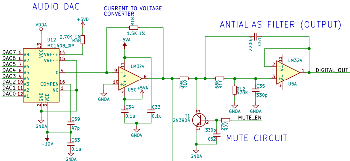
Next, the signal goes through an op-amp circuit which mixes the digital sound with the audio from the FM synthesis chip as well as the CMS chips. Unlike later Sound Blaster cards, the mixer is fixed and cannot be adjusted.

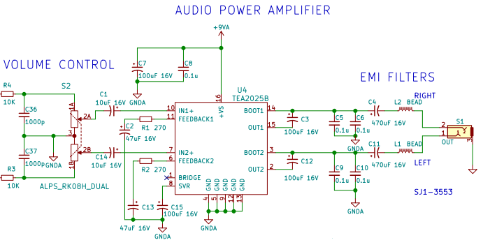
Finally, the signal goes through the volume control wheel and the built-in audio speaker amplifier before coming out the audio jack on the back of the card.

Since there is only one DAC, playback is mono, not stereo.

Audio Input
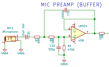
The Sound Blaster has a microphone jack on the back. It is only compatible with dynamic microphones or electret microphones that have built-in batteries because it has no bias power supply, unlike more modern sound interfaces. The input signal goes through a series DC-blocking capacitor and then into a preamplifier that converts the high impedance microphone signal into a low impedance signal needed by the rest of the internal circuit.
The preamplifier is also a Sallen-Key low-pass filter with a cutoff frequency of 4KHz. It is a 2nd order filter which means the attenuation increases by 40dB per decade. At 40KHz, the signal is down by 40dB.

The signal passes through a gain stage that amplifies the low-level signal, then passes it into the AGC (Automatic Gain Control) circuit. This circuit rectifies the AC input signal and filters it into a slow-moving voltage that represents the average level of the output (an envelope signal). This signal goes into a transistor that can attenuate the gain stage’s input signal level if it gets too high.

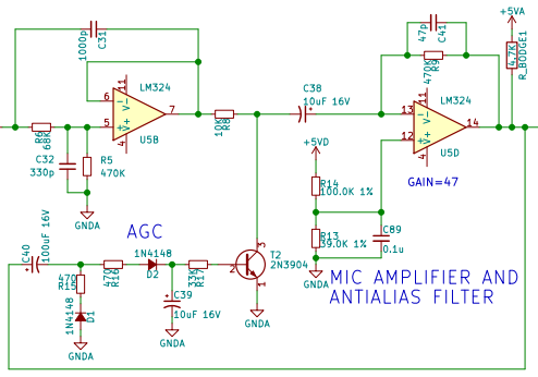
The gain stage uses an LM324 with a gain of 47 (about 17dB). Looking at the LM324’s datasheet, that gives us a bandwidth of about 30-50KHz. A small feedback capacitor (C41) makes this amplifier a single-pole low-pass filter with a cutoff frequency of 7.2KHz.

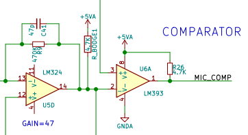
This filtered and amplified input signal goes into one input of the ADC comparator. The other comparator input comes from the audio DAC which generates the successive approximation signal.

There is something missing from the circuit, however. A true successive approximation ADC uses a sample-and-hold circuit to prevent the signal from changing voltage during an acquisition cycle. The Sound Blaster cheats and just pretends that the antialiasing filter will slow the signal down enough. It’s probably a bit noiser than it could be.

During ADC sampling, the DSP activates a mute circuit that prevents the successive approximation signal from bleeding out into the speakers, which is important because it would sound terrible! Because the audio DAC is used for both playback and recording, the Sound Blaster is only half duplex and cannot play back audio at the same time it is recording it.

MIDI I/O
The DSP, since it is just an 8051, has a built-in UART. The DSP firmware configures the UART for the MIDI baud rate (31250) and handles the MIDI messages.

There is a jumper bank just above the DSP that has some wires installed instead of a normal 0.1″ header pin array. The shorting wires route the UART RX and TX lines from the DSP out through the joystick connector. If the wires were removed, then a serial cable could be installed on the headers. I suspect this is how the engineers at Creative Labs debugged firmware issues.

To use the MIDI I/O with standard MIDI devices, you have to use a special adapter cable that includes the optoisolators required by the MIDI standard.

FM Synthesis
Two Yamaha chips produce FM-synthesized sound. The famous YM3812 OPL2 chip generates a digital serial PCM signal that gets converted into an analog waveform by the YM3014B DAC. The OPL2 chip has already been described extensively elsewhere.

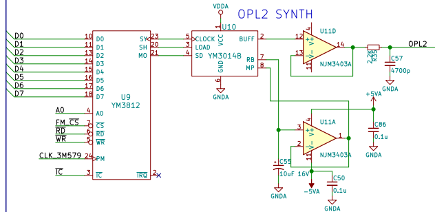
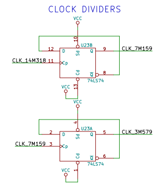
One interesting thing is that the Sound Blaster uses two daisy-chained flip-flops to divide the ISA bus’s 14.318MHz clock signal down to 3.579MHz for use by the OPL2 chip.

To sum up, this part of the Sound Blaster behaves exactly like an Ad Lib sound card. Since there is only one single-channel YM3812, the FM synthesis output is mono.

CMS Music
The CMS (Creative Music System) chips are actually Philips SAA1099 audio chips.

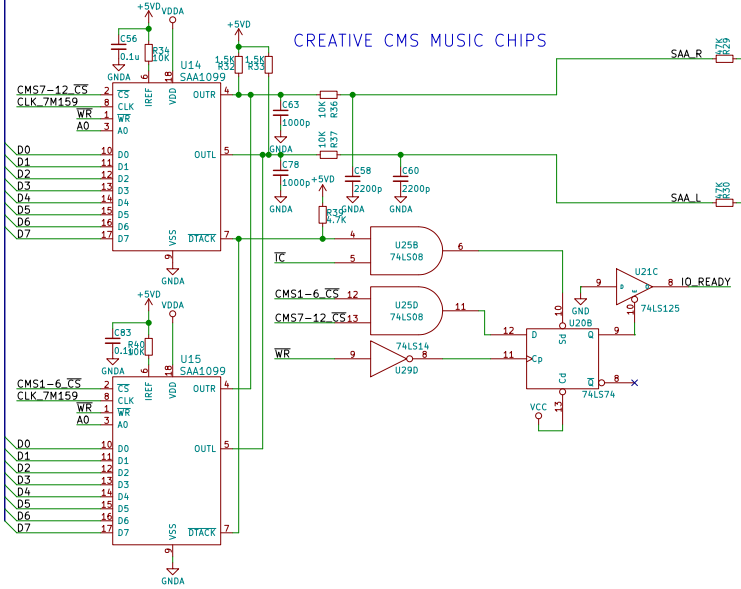
The clock signal for these chips comes from a 7.159MHz signal which is just the ISA 14.318MHz clock divided by two. It’s a tap off the same clock divider chain used by the FM synthesis chip.

These two chips generate a left and a right channel, and they’re the only source of stereo sound on the Sound Blaster!

There is a flip-flop, U20B, that drives the ISA bus’s IO CHRDY signal to lengthen the host PC’s bus write cycle for the SAA1099 chips because they are quite slow.

Joystick Circuit
Here’s another place where the Sound Blaster cheats and doesn’t use an analog-to-digital converter. Just like the IBM joystick card (and clones), it uses an NE558 (the “quad” version of the classic 555 timer) as a variable one-shot timer. Each joystick axis is a variable resistor, that, along with a fixed capacitor in the Sound Blaster, controls a time delay. Writing to the joystick port triggers all four timers (one per joystick axis). The software then polls the joystick port and times how long it takes for each axis to reset. The time delay correlates with the position of the joystick.

In the above capture, the circuit has been connected to a resistance of 38.1K. Since the fixed capacitor is 0.01uF and the 558 threshold voltage is 2/3 of 5V or 3.33V, we get a time delay of about 420us.

Conclusion

The Sound Blaster 1.0 met a market need for a low-cost sound card with lots of features and backwards compatibility. It supported digital sampling using some clever hacks to keep the costs down, worked with all existing software that supported the Ad Lib sound card, and even integrated joystick support and MIDI functionality. No wonder the Sound Blaster series became the most popular sound card of all time!

If you want to try one out in your retro PC, consider building my replica design, the Snark Barker. The design files are available at my GitHub repository.

A Miniaturized Discrete MC1466

Cleverness, Projects 15 Comments

Update: the bill of materials is now available. You can order boards from OSH Park using this direct link. Last time I ordered, it cost me a grand total of $3.55 for three boards (free shipping), and it took about two weeks for the boards to arrive.

I screwed up. My bench power supply is a Lambda LPT-7202-FM triple output (0-7V @ 5A, 0-20V @ 1.5A, 0-20V @ 1.5A), and I blew it up by trying to desulfate a lead-acid battery. The idea is to take a dead lead-acid battery and recondition it by charging it with a current-limited 15V source while feeding it high voltage pulses. I had a diode connected in between the battery and the bench supply to protect the power supply from the high voltage pulses. Well, the diode failed. It was a sad day.

Fortunately the service manual for the supply is available online. I traced around the circuit and found that two of the power control chips were fried, but everything else seemed OK–I could move the one remaining functional chip from channel to channel to confirm that. The control chips were marked with the Motorola logo and a Lambda house part number: FBT-031. A forum thread indicated that the part was actually the MC1466. Sadly this chip is long out of production and a bit hard to find, although a popular auction site had several listed from a seller in China (but who knows if the parts were counterfeit or not).

The datasheet has the full schematic including resistor values, but how do I know that it actually matches the chip? Since the IC is packaged in a ceramic DIP, I followed reader Uwe’s suggestion and took a chisel to one of the dead parts.

It worked and nothing was damaged! The die looks like this:

I went over the layout and it matches up with the datasheet schematic. Those funny round elements are actually zener diodes. You can see the long skinny resistors and the lateral PNPs as well as the NPN transistors and diodes. Below is the schematic (click to enlarge):

The IC design is pretty archaic. I’d say it dates to the late 1960s. There are fairly ordinary differential amplifiers, but the current mirrors are really strange, and the voltage reference circuit uses Zener diodes and series-connected diodes instead of a temperature compensated bandgap reference. The two Zener diodes (the only round features on the die) are probably just reverse biased NPN transistors, using the ~7.5V avalanche breakdown of the base-emitter junction. The lateral PNPs have a much higher breakdown voltage so they can’t be used this way.

Here’s a labeled die photo (click for a larger image) so you can see where each of the components are. The component designators match up with my schematic, not the IC datasheet schematic.

The device is simple enough that I decided to build a really small PC board with discrete components. I found that the BC847BVN (NPN/PNP dual transistor), BC847BV (dual NPN), and BAS16VV (triple diode) came in a really tiny SOT-563 package. Believe it or not, this is not the tightest or smallest layout I’ve done. This is a 2-layer board with 6 mil traces and 6 mil spaces.

To give you an idea just how small the SOT-563 is, take a look at the first BC847BVN I soldered:

The part is 1.05mm x 1.05mm! I had to use a very fine soldering iron tip and a microscope. Another trick is to use really thin solder (I used 0.38mm). As you can see, the resulting board is just slightly larger than the original DIP IC:

It really is pin compatible. I plugged two of them into my Lambda supply and now it works perfectly!

Mel, Blackjack, and the LGP-30

Cleverness No Comments

A friend passed on the following articles regarding a rather famous hack:

https://news.ycombinator.com/item?id=7869771
http://www.jamtronix.com/blog/2011/03/25/on-the-trail-of-a-real-programmer/

The LGP-30 was an early computer manufactured in 1956 and sold by the Royal McBee division of the Royal Typewriter Company. It had 113 vacuum tubes, 1450 diodes, a magnetic drum memory, and an oscilloscope screen with a template marking the register bits (instead of the more traditional panel with blinking lights). Mel wrote a lot of code for this machine, including a blackjack demo program, entirely in raw machine code, taking advantage of various quirks in the machine to keep the program very compact.

The Jamtronix blog has a link to a purported paper tape dump of Mel’s program.

Foolishly I decided to figure out the paper tape dump. I succeeded, and it looks like it’s in a format that a bootloader was supposed to understand, but not the bootloader documented in the LGP-30 manual. So first I ran the raw file into a popcount routine to see what the most common letters were. It was a subset of the alphabet, but had all the numbers except for the number ‘1’.

Wat?

Back then they did a few strange things. One of them was using the lowercase letter ‘L’ as the number 1. Right. Also, since the LGP-30 was hexadecimal, they used extra letters to represent numbers beyond 9, but instead of using a-f, they used fgjkqw.

Then the single quote ‘ is used as a record delimiter, and the letter ‘v’ at the beginning of the block of records identifies the track and sector where the data is to be loaded. Each block has 64 words, 8 per line (which fits perfectly in a single track on the magnetic drum memory). To save space, they omit leading zeros, so incoming characters of 4 bits each are shifted left 4 at a time. At the end of the block is a stray word whose purpose I cannot figure out. I suspect it’s a parity or checksum, but it doesn’t match a simple checksum of all the data.

This machine’s architecture is a clever nightmare. Self modifying code was encouraged and was the standard way to accomplish common tasks. For example, to branch to a subroutine, you do this:

1000: r 3050     <- Set up return address by writing PC+2 to the destination address of the instruction at 3050.
1001: u 3000     <- Unconditional branch to address 3000.
1002: ...        <- Magically we pop up back here!
...
3050  u 0000     <- Looks like a unconditional branch to location 0 right? No, it's just a placeholder address. Yay, we can do without a link register!

And Mel coded this up in machine code. Probably because the “assembly” mnemonics are not particularly helpful, he must have quickly memorized the opcodes themselves. And why did he use instructions as data? The machine doesn’t decode the upper 12 bits of a word, so if you didn’t use it, it was just wasted. Basically the architecture of the machine naturally led Mel down this slippery slope.

So you might think that Librascope/Royal McBee, based on customer feedback for this machine, must have simplified the design for a later machine, the RPC-4000. And you would be wrong–it’s even worse…

Anyway, here’s my disassembled version: blackjack.txt. The track number is listed first, once for every block. In each block, every line has the sector number first, followed by the instruction mnemonic, following by the track and sector numbers of the instruction’s target. After that are the raw bits. The first two instructions are clear instructions followed by an unconditional branch. This goes to track 49 sector 34. You can follow the instruction flow from there.

As for me, I’m going to stop now before I accidentally learn how to program the LGP-30.


Oscilloscope Video Monitor

Cleverness, Projects 12 Comments

Watch this YouTube video, and then read the rest of the post.

So how did I do it? It is actually a very simple circuit.
Basic Ramper Schematic

The LM1881 separates the sync signals from the NTSC composite video coming from the camera. It outputs a vertical sync signal (active low) that asserts during the vertical retrace period and a composite sync signal (also active low) that asserts during the horizontal retrace period and also during the vertical retrace period (but with a set of serration and equalization pulses).

To connect these to my oscilloscope, I have to use the XY mode on the scope and convert the sync signals into deflection signals. This is done using analog ramp generators. The simplest way is to use an RC circuit to generate a rather nonlinear ramp. When the sync signal goes high, it charges the capacitor through the resistor. When the sync signal goes low, the diode allows the capacitor to discharge immediately. This generates the sawtooth waveform. Adjust the R value so you get the most complete ramp (goes most of the way up to 5V).

The video signal is fed directly into the Z-axis signal at the back of the scope. Because the Z-axis signal has the opposite polarity from regular video (it is a blanking signal, where a positive voltage will turn the beam off), I had to build a really basic video buffer to invert the signal. This is a nice exercise in transistor biasing using four external resistors. Don’t ask me for the schematic–you should try to build it yourself. Even if you don’t get it working properly right away, you’ll discover all sorts of interesting analog video effects!

Point Contact Transistor

Cleverness 2 Comments

My friend Jeri Ellsworth recently figured out how to make a point contact transistor by cracking open a germanium diode. It looked pretty straightforward so (deviating from this blog’s usual content) I took a crack at it myself:

Point Contact PNP

The original diode contact serves as the emitter connection. The base is the chip of germanium that is visible in the bottom part of the diode (with the stripe). The collector is a piece of phosphor bronze wire I pulled off the end of a guitar string. I sharpened it to a point with a Dremel sanding wheel and soldered it to a piece of bare wire to make it easier to handle.

The fine-pitched screws are used to maneuver the wires into contact with the block of germanium.

The germanium base is actually n-doped. To create the collector junction, you have to create p-doped regions. One crude way to do this is to apply a burst of current across the reverse-biased junction (positive voltage to base, negative voltage to collector). I don’t know if the mechanism is thermal or electrical, but phosphorus from the phosphor bronze wire gets carried into the germanium, creating the p-type region. For this experiment I used about 200V on a 10uF capacitor, and I discharged it into the junction through a 1K resistor. Jeri originally used something like 20V but I read in a paper several hundred volts were usually used for this purpose.

Jeri used an oscillator circuit to test her transistor, but I got lazy and just put it in a simple inverting amplifier circuit. At first the transistor didn’t work (output was in phase with the input) but after some tweaking of the wires, the output finally went 180 degrees out of phase. This is an absolutely terrible transistor, and the gain is really too low to consider this a transistor.

Point Contact PNP - Inverting Amplifier In/Out

I’m going to play around with it a bit more to see if I can improve the gain…

Modifying an AC Adapter’s Output Voltage

Cleverness, Projects No Comments

My IEE clock runs on about 6.5VDC. Why the odd voltage? There are sundry voltage drops throughout the circuit that require the power supply voltage to be higher than the 6V rating for the light bulbs. The problem is that you just can’t find 6.5V AC adapters.

Fortunately it’s quite simple to modify an existing AC adapter to run at the new voltage. I’m sure there are other people who might want to get their own custom output voltages, so here’s a short tutorial.

Disclaimer: if you go ahead with this project, you’re doing it at your own risk. AC line voltage is quite dangerous and you could be injured or even killed. If you get shocked, get medical attention right away: there have been people (often with a previously undiagnosed heart condition) who have received a “small shock” only to drop dead a couple of hours later.

Here is what you need: A switching AC adapter, a flat screwdriver, a soldering iron, an assortment of surface mount resistors, and some time. It is important that the AC adapter is of the new switching style rather than the old transformer style–usually you can tell if the AC adapter feels light and is small enough not to block adjacent outlets, yet has a relatively high current rating for its size. I am starting off with a fairly generic 5V 2 amp AC adapter. Yours will likely use a similar circuit inside.

Quick side note: Why are the new AC adapters so much smaller? First, to provide a given amount of power, a transformer (copper windings around some type of core material) has a physical size that decreases as the frequency goes up. A transformer designed to operate at 60Hz or 50Hz  is going to be much larger than a transformer that is designed to operate at 15KHz. Since the frequency of the AC line is fixed, these new AC adapters work by converting the input AC to a much higher frequency. There is also a little circuit that looks at the output voltage and tweaks the converter circuit to maintain a constant output voltage. Thus, the new AC adapters have much better regulation than the old styles. As an added bonus, this type of design can operate at 50Hz, 60Hz, 120V, or 240V! To get into more detail, there is a feedback circuit that compares the output voltage to a voltage reference, then sends an error signal to the converter circuit at the primary side of the transformer. The error signal is isolated (for your safety) using an optocoupler.

To take apart the AC adapter, crowbar the plastic halves of the case where they meet in the middle. Try to find the little plastic catches that keep the halves together. You might need two screwdrivers to get them to come apart. Inside you can see a little circuit board with components and some wires.

Modifying an AC Adapter

To modify the output circuit, the feedback circuit must be modified. I sketched out the circuit and learned that this particular AC adapter uses a clone of the TL431 reference+error amplifier circuit (which is the weird zener-diode looking thing in the photo above). This particular device, the AM431, has an internal 2.495V reference. The output voltage is divided down so it can be compared with 2.495V, and this is done with a resistive divider formed by R1 (4.87K) and R10 (5.23K). R10 goes to the output voltage, and R1 goes to ground. In this design, I can only modify R1 since R10 (acting in combination with the feedback capacitor) also determines the loop compensation pole (no need to mess with this). Based on my reverse-engineered schematic of the secondary side, the formula for the output voltage is Vout = (1 + R10/R1) * 2.495. Replacing R1 with a 3.3K resistor should bump up the output voltage.

It’s easier to remove a surface mount resistor using two soldering irons, but if you only have one, you can blob a bunch of solder on top of the resistor to wet both sides, and then flick it off with the iron. Be careful to get rid of any splattered solder since it could cause some dangerous short circuits.

You can test it before putting the case back on by plugging it into a power strip that has a circuit breaker and a switch–turn it off first! Connect a multimeter to the outputs with alligator clips, and use one hand to switch on the power and check the voltage. If you want to be a little extra safe you could plug the power strip into a GFI outlet. The safest approach (especially if you want to take measurements on the AC line side of the isolation barrier) is to connect the whole rig to an isolation transformer. Once you’ve confirmed that it works, put the case back together and mark the label with the new output voltage. If the output voltage is higher, you will need to decrease the current rating proportionally. If you’re decreasing the output voltage, you shouldn’t increase the current rating since internal components may have a pretty low maximum current capability.

If you want more information about the TL431 (which is a really neat little device that could be useful for lots of other circuits), check out this application note: Designing with the TL431.

Nixie Tubes!

Cleverness 1 Comment

Recently I purchased a number of nixie tubes from the local electronics flea market:

Nixie Tubes

A few of them caught my eye. This Burroughs B-5448 one was most likely used in a calculator or possibly a meter to indicate plus and minus as well as the overload condition.

Burroughs B-5448 Nixie

And this National NL-989 was used for indicating the unit or mode of a multimeter. There are two “partitions” in this nixie tube: one contains the symbols “A”, “M”, and “K”, while the other contains “C”, “V”, and “Ω”. The multimeter would have used this to indicate “AC”, “MV”, “KV”, “MΩ”, “KΩ”, and so on.

National NL-989 Nixie

Notice how the glow is a different color in each tube? My camera did an excellent job of reproducing the correct color, so what you see is very close to what the ionized gas actually looks like. The National tube appears to contain mostly neon, while the Burroughs shows light blue “fringing”, indicating the presence of mercury, which was used to increase the lifespan of the tube.

RCA 6499 Radechon

Cleverness No Comments

At the electronics flea market I found a rather interesting-looking vacuum tube. It appears to be a CRT but with a metal cap at the end.
Radechon

As it turns out, this device is a memory which could have been used in some old computers, storing around 16 kilobits. It could also have been used in radar systems for converting polar coordinate-based sweeps to raster sweeps (like a TV). The socket end contains an ordinary electron gun like the one found in a CRT, but the front end does not contain the usual phosphor screen. Instead, there is a 1mil thick sheet of mica with a fine grid of wires laid on top. On the other side of the mica there is a metal plate.
Radechon
Here’s a closeup showing the metallic screen on the front. The mica underneath capacitively stores electrons that are laid down by the electron beam. This memory can store analog waveforms since higher voltages are represented by a higher density of electrons at a particular spot, and lower voltages correspond with a lower electron density.
Radechon

Data for the tube is available from David Forbes.

Here are a couple of other sites with information:

Åke’s Tubedata

World Power Systems

Virtual Valve Museum

Cold War Infrastructure (A full-page RCA ad for the device)

Coby DP-151SX Hacking – LCD Extraction and Interrogation

Cleverness, Projects 21 Comments

In this previous post I disassembled the Coby DP-151SX digital picture frame. This device is very hackable, and includes a lot of goodies such as a Li-Ion battery and battery charger circuit as well as a neat little color LCD display with a white LED backlight. The pinout for the LCD is in the previous post.

The MAXQ2000 microcontroller development board I have uses a 0.1″ spacing header to connect to the I/O pins, so I made a little adapter and wired it up to the LCD connector using wire-wrap wire. It uses 13 I/O lines, but that could be reduced 11 if CS# is wired to ground and RST# tied to a separate reset IC (such as a MAX811). It’s actually a good idea to use CS#, because you can then multiplex the functionality of all the other pins and recover that I/O.

Here is a picture showing the LCD up and running with a simple test pattern:
Coby DP-151 Photo Keychain - LCD Extraction and Interrogation

It’s not 128×128, but actually 132×132 pixels. The color depth is 16-bit using a fairly standard 5-6-5 bit encoding. See the PCF8833 datasheet for more details.

Spark Fun has a similar LCD display which uses the same controller, only it costs $20. Amazon.com sells the Coby-151SX in black for $10. Not a bad deal: for $10 less you get a Li-Ion battery, mini-USB cable, and a driver CD, which you could use as a coaster for your Mountain Dew to help with the LCD programming. Spark Fun has some sample code which you should easily be able to adapt for parallel mode (since the Coby LCD connector brings out the parallel data lines, unlike the Spark Fun LCD).

The source code for my test program will get posted once I clean it up and possibly add functionality (Character fonts? Bit blitters?)

Vietnamese iPhone 3G Hacking

Cleverness No Comments

CNET’s Crave has a really fascinating post about a gentleman in Vietnam who has figured out how to unlock 3G iPhones–as of this writing, there is no software way to unlock this phone.

Unlocking iPhone 3Gs–the Vietnamese way

There are some interesting pictures showing some methods used by the Vietnamese technicians to remove and replace the flash memory device. They use a cheap hardware store heat gun, which is normally used to strip paint, to heat the solder until it melts, and then they remove it with tweezers. One of the problems with this sort of rework is that the adjacent components often loosen and shift or even fly off completely.

Look at the last picture in the article. The technician is using some small metal plates to protect the other components from the blast of hot air. Genius!