IEE Clock Internals
April 28, 2010 5:53 pm Clocks, ProjectsLet’s take a look inside the previous posted IEE clock:

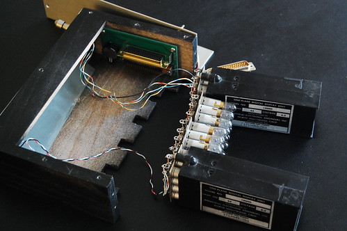
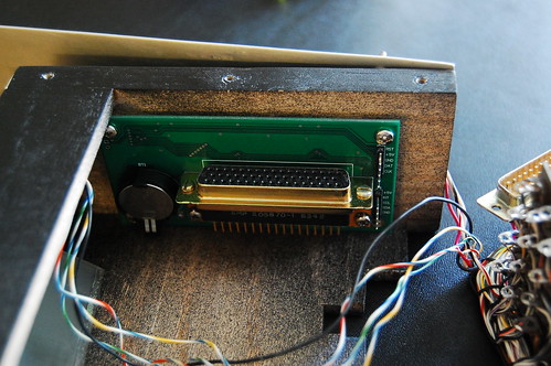
Here you can see the laced wiring harness for the displays. This is not a multiplexed display–each of the 40 light bulbs has its own transistor driving it. All these wires come off the displays and into a very large DIN-style connector that plugs into the main circuit board. The ICs are all on the other side of the board.
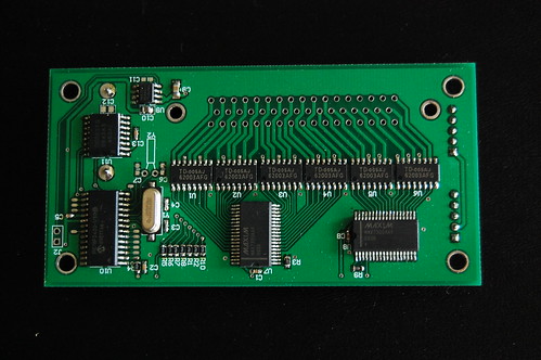
This is a closeup of the main PCB. It’s quite small. You can see the PIC’s ICD header off on the right, along with a header that allows access to the I2C bus for troubleshooting.
And looking at the other side, we can see the driver ICs, the PIC, and the RTC device, along with some passives. You can also see the spare pads I put next to the PIC so that I can easily solder wires to the unused GPIOs if I ever need them.
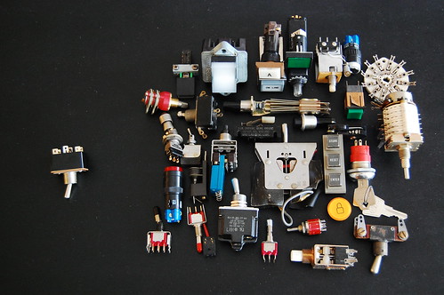
Some people commented about the switch on the front. I have a decent collection of switches of all colors, types, and vintages. It’s disconcerting for me to see what would be a really neat project marred by boring switches. Here’s a small sampling of my collection:
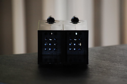
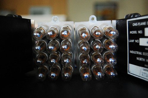
People really liked the photos of the disassembled IEE module from the other website. Here are a few gratuitous “artsy” shots: