Point Contact Transistor
November 5, 2010 Cleverness 2 CommentsMy friend Jeri Ellsworth recently figured out how to make a point contact transistor by cracking open a germanium diode. It looked pretty straightforward so (deviating from this blog’s usual content) I took a crack at it myself:
The original diode contact serves as the emitter connection. The base is the chip of germanium that is visible in the bottom part of the diode (with the stripe). The collector is a piece of phosphor bronze wire I pulled off the end of a guitar string. I sharpened it to a point with a Dremel sanding wheel and soldered it to a piece of bare wire to make it easier to handle.
The fine-pitched screws are used to maneuver the wires into contact with the block of germanium.
The germanium base is actually n-doped. To create the collector junction, you have to create p-doped regions. One crude way to do this is to apply a burst of current across the reverse-biased junction (positive voltage to base, negative voltage to collector). I don’t know if the mechanism is thermal or electrical, but phosphorus from the phosphor bronze wire gets carried into the germanium, creating the p-type region. For this experiment I used about 200V on a 10uF capacitor, and I discharged it into the junction through a 1K resistor. Jeri originally used something like 20V but I read in a paper several hundred volts were usually used for this purpose.
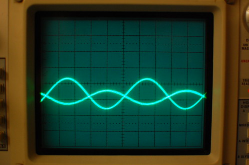
Jeri used an oscillator circuit to test her transistor, but I got lazy and just put it in a simple inverting amplifier circuit. At first the transistor didn’t work (output was in phase with the input) but after some tweaking of the wires, the output finally went 180 degrees out of phase. This is an absolutely terrible transistor, and the gain is really too low to consider this a transistor.
I’m going to play around with it a bit more to see if I can improve the gain…


