
A MOnSter Mystery, Solved
July 7, 2016 10:01 pm MOnSter 6502I brought up an additional MOnSter6502 board today. At first it failed my basic validation routines, tripping up on the LDA nn,Y instruction ($B9).
The bus diagnostic output showed that LDA nn,Y was trying to read nn+Y+1 instead of nn+Y (in my test, it accessed $0211 instead of $0210). The LEDs showed that the Y register contained the expected value, so I thought the ALU carry in signal may have been loading a ‘1’ instead of a ‘0’, thus causing the incremented value. I scoped it out and it was fine.
Then I noticed that LDA nn,X worked fine which is totally weird because those instructions are just about identical! So I physically inspected the Y register and saw this tomfoolery:
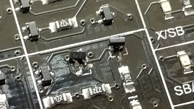
Those transistors are in bit zero of the Y register. The one on the left prevents anything but a ‘1’ from being in the LSB. The one on the right was supposed to drive the LED on so that I could tell the bit was stuck, but it decided to cover for its dead buddy. I don’t even know how this happened. It could have been shipping damage, or maybe I fat fingered a screwdriver.
After fixing it, the board worked fine. Two dead transistors and a lying LED. Gotta love transistor level debugging.
Richard :
Date: July 19, 2016 @ 9:11 am
Good find! Sometime, you just don’t know your own strength!
Bill Seiler :
Date: April 10, 2017 @ 7:12 pm
I would love to get a Monster 6502 to give to Chuck Peddle on his 80th birthday!
42Bastian :
Date: May 24, 2017 @ 7:41 am
Great, transitor-level debugging. This is pure bare-metal.
Artur :
Date: May 14, 2018 @ 10:28 am
Hi Eric,
how do these three transistors (where the right is for the LED) store one bit? In NMOS logic you need two transistors for a single NOR gate. This is not even a latch and yet stores one bit of information?
What transistors do you use? I want to build the Scott CPU in the same fashion like you build the Monster. A colleague of mine told me that I must pay much attention to the voltage peaks on the gate during powering up the system, since it can destroy the transistors. He suggested to put resisitors in front of the gates, which would slow down the processor even more. The resistors you use are just for NMOS logic, am I right? So how did you tackle this powering up issue?
Greetings from Germany
Artur
PS: great job!
PPS: you are a crazy monster 🙂
eric :
Date: May 22, 2018 @ 10:32 pm
Artur, the design uses dynamic NMOS. It means that you can create a dynamic latch by using (at minimum) a single transistor. The bit is stored in the gate capacitance, just like it is on a DRAM chip. This works well for a latch that gets written to every clock cycle. For those latches that are not, you use two transistors to create a buffer (two inverters one after another) and the third transistor to create a pass gate that will take the output of the latch and feed it back to the input.
The transistor selection depends on a lot of factors. I just went and looked for low threshold voltage, low gate capacitance FETs. If the VGS(max) rating is high enough (10-20V) and your traces are short then you should not have to worry about voltage transients. I have resistors in my design but they are just replacements for the depletion mode MOSFETs in the original IC.