A MOnSter Mystery, Solved

MOnSter 6502 5 Comments

I brought up an additional MOnSter6502 board today. At first it failed my basic validation routines, tripping up on the LDA nn,Y instruction ($B9).

The bus diagnostic output showed that LDA nn,Y was trying to read nn+Y+1 instead of nn+Y (in my test, it accessed $0211 instead of $0210). The LEDs showed that the Y register contained the expected value, so I thought the ALU carry in signal may have been loading a ‘1’ instead of a ‘0’, thus causing the incremented value. I scoped it out and it was fine.

Then I noticed that LDA nn,X worked fine which is totally weird because those instructions are just about identical! So I physically inspected the Y register and saw this tomfoolery:
IMG_20160707_123730
Those transistors are in bit zero of the Y register. The one on the left prevents anything but a ‘1’ from being in the LSB. The one on the right was supposed to drive the LED on so that I could tell the bit was stuck, but it decided to cover for its dead buddy. I don’t even know how this happened. It could have been shipping damage, or maybe I fat fingered a screwdriver.

After fixing it, the board worked fine. Two dead transistors and a lying LED. Gotta love transistor level debugging.

MOnSter 6502 Runs BASIC!

MOnSter 6502 No Comments

Where we left off, the MOnSter 6502 had successfully ran a basic validation suite that validated a subset of the instructions but checked every bus cycle for accuracy. Shortly afterwards I was able to get it to run the full validation suite.

BASIC ran just fine after that. It was quite slow with a 6KHz clock but it was enough to run some simple BASIC programs. Typing was difficult because my validation computer uses an Atari POKEY chip to scan the keyboard, and it latches keystrokes very slowly because of the slow bus clock.

I’ve been experimenting with increasing the maximum clock frequency. It helped to reduce the bus capacitance that I added, but if I went too low, it cut into the minimum operating frequency. With less bus capacitance I was able to get the clock up to about 60KHz, and BASIC is quite usable at this speed.

There is an issue I’ve been running into that has to do with the active bus pullups. The pullups are switched on by CCLK (first clock phase), and the pulldowns are normally changed on the CP1 edge (second clock phase). However this is done using a dynamic latch, so if the clock slows down too much, the latch will change state, causing both pullup and pulldown to be turned on at the same time. Here’s an example circuit:

PullupIssue


The circled node is the storage node of the dynamic latch. If CP1 is off for too long, then this node can discharge, going from a ‘1’ to a ‘0’.  When that happens, the output goes high and drives a ‘1’ into the pulldown transistor when CCLK goes high. CCLK turns on the pullup at the same time. As you can see in the diagram, I’ve added a small resistor in between both transistors to limit the current.

This resistor, although it protects the transistors, also limits the maximum clock speed by limiting how fast the bus capacitance can charge up.

I’ll be experimenting with some alternative ways of protecting the transistors without slowing down the bus too much.


MOnSter 6502 Bringup Status

MOnSter 6502 1 Comment

Wow, Maker Faire was totally nuts! Lots of people came by to check out the MOnSter 6502 and I had some interesting conversations with people. After taking a few days to recover, I dug back into the bringup and validation process.

The MOnSter 6502 now passes my basic validation test suite. I discovered two problems.

It was not booting consistently, and kept getting stuck in a bad state where the ‘1’ bit would run off the end of the instruction sequencer, or it would get stuck in a loop running the same (wrong) instruction over and over again. The RESG latch also was stuck on.

When RESET goes low, it turns on RESG. This forces the BRK instruction (which is meant to trigger a software interrupt) into the predecode IR (instruction register) by deasserting D1x1, sets the vector address to the reset vector (instead of the IRQ vector, as BRK normally does), and prevents BRK from writing to the stack so it can’t push the program counter and status bits. When BRK is done, it clears the RESG latch. This is a very clever hack that the original designers used so they could avoid having to run a reset line all over the chip.

Oddly, even when RESG was set (I could tell by a convenient LED), the contents of the IR were not all ‘0’ (again, according to convenient LEDs). Turns out the quad FET array devices used in the IR had some leads that were not soldered down correctly. Fixing that solved the problem.

After trying to run the validation suite again, it started failing the cycle-by-cycle validation on the first time an actual BRK instruction was supposed to be executed. BRK saves the least significant byte of the program counter the most significant byte, and finally the contents of the status register to the stack (with the B bit set so your interrupt service routine can tell the difference between BRK and a hardware IRQ). In this case, it was writing the most significant byte and the status register to the wrong locations in memory.

So I hard-wired the PHA (PusH Accumulator) instruction onto the data bus so I could observe a very simple instruction write to the stack. The value was written correctly, but instead of decrementing the stack pointer by 1, it subtracted 18! PHA decrements the SP by loading it onto the ADL bus and setting the ALU to add with the B input hold register connected to ADL and the A input hold register connected to the special bus. The idea is that by adding $FF you decrease the value by one. This only works if nothing else is driving the special bus except for the precharge pullup MOSFETs. It’s another clever hack from the original 6502 designers. In my case, instead of seeing $FF, the ALU was latching $EE! I tried adding a small amount of capacitance from special bus lines 0 and 4 to ground to keep the voltage up from the precharge cycle, and PHA then worked correctly. I ended up adding capacitors to all the bus lines just in case.

After those fixes my basic validation test suite passed without any further issues.

The next step is to run a more complete set of validation tests, and then BASIC!

The MOnSter 6502

MOnSter 6502 16 Comments

So, I made a thing. A really big thing. Really big and really crazy.

You might have seen my discrete 555 and 741 IC electronics kits. Well, a while back I had this idea about creating a discrete version of a microprocessor, but it just sounded too difficult, time consuming, or impractical. And part of me didn’t want to do it, because it just sounds so tedious to design–at every stage, I was secretly hoping to find a show-stopping problem. But part of me was really interested to see if it could be done.

At dinner, Windell and I went through a thought experiment to see if it would even be possible. We weren’t sure how many transistors were in a 6502 (more than 1,000 but less than 10,000). If four surface mount transistors can fit in a square centimeter, then the board would need to be about 1,000 square centimeters, or about 32cm (13in) on a side, which is not as huge as we originally thought. Darn it, time to investigate further!

The hard work of reverse engineering the actual 6502 has already been done by the folks at Visual6502.org. I was able to extract the netlist from their Javascript simulation, which contains a list of all the transistors and every single wire connecting them together.

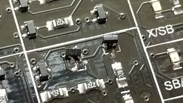
The 6502 uses dynamic NMOS logic, so it has a large number of “transmission gate” transistors that are used to switch currents. For various technical reasons, only a 4-terminal MOSFET can make an effective NMOS transmission gate. Those are really hard to find (nearly all MOSFETs are 3-terminal devices), but I found one–it’s an array of 4 MOSFETs on a single chip with a separate substrate pin.

I ran simulations using the transistors I found, and noticed that basic combinational logic and latches worked. I ordered parts and prototyped a few circuits. They worked perfectly.

I designed and ordered an OSH Park circuit board with just 8 bits of the program counter register. I thought to myself that there was no way such a complex circuit could work, especially with the ripple carry propagation. Well, it worked.

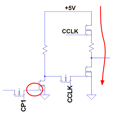
It was time to bite the bullet. I wrote a Python program that turned the Visual6502 netlist into a 3,510 line spreadsheet, and I began entering (on July 3, 2015) the transistors one by one into the schematic, highlighting each transistor as I finished it. Along the way, I noticed that the Visual6502 netlist had three extra transistors, T1088, T1023, and T3037.

(An example of an extra transistor)

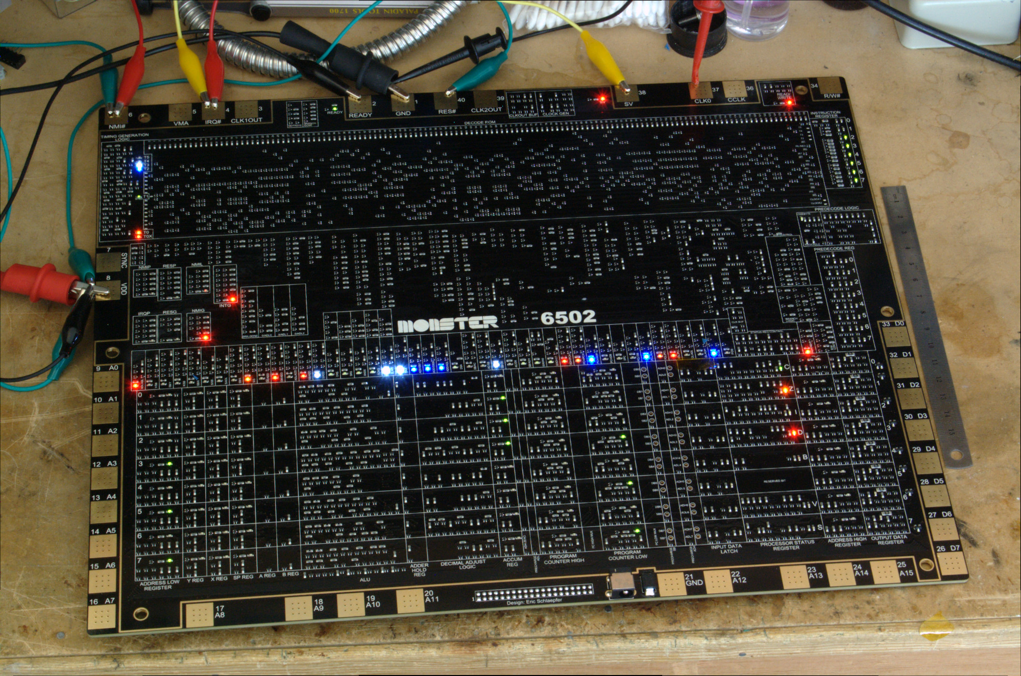
When I was done with all 61 pages, I wrote another Python program to compare my schematic against the original netlist and corrected a few mistakes. Then I added 167 colorful LEDs to various control lines and data bits, and a few protection components.

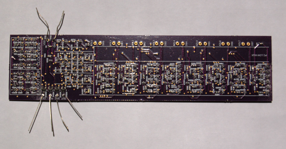
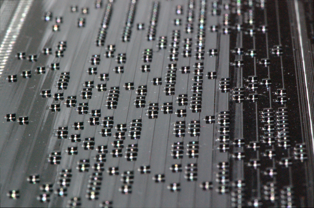
The layout came next. In the layout software, I placed 4,304 parts by hand and wired them up manually (no autorouter) over the course of several months, finishing the last transistor on Dec 1, 2015.

And last Thursday, the first boards came in. They are beautiful!

We’ll be bringing it to Maker Faire, so I have a week to work on bringup testing. Wish me luck!

You can find more details on the main project site, monster6502.com.