Maker Faire 2017
April 22, 2017 Uncategorized 4 CommentsThe MOnSter6502 will be at the Bay Area Maker Faire this year! If you’re around, come by and say hi.

The MOnSter6502 will be at the Bay Area Maker Faire this year! If you’re around, come by and say hi.
Edit: Someone who goes by W9EO has recorded assembly videos on YouTube which you may find helpful for building this card. He is also selling completed cards if you don’t want to solder it yourself.
Growing up, I used to play some games on an AST 286 computer, including Commander Keen, Wing Commander, and a few others.
Sound in those days was primitive compared to modern machines, but I still have a soft spot for the bleeps and bloops of the OPL2 synthesizer cards (which includes the AdLib).
Recently I have been fixing up an IBM XT (with original CGA card!) and I needed a sound card. It turns out that early sound cards like the AdLib or the Sound Blaster are quite expensive on the used market, so I thought I’d make a clone of the AdLib sound card (1990 version). Being me, I couldn’t just make an electrical equivalent. It had to look as close as possible to the real thing.
Here it is.
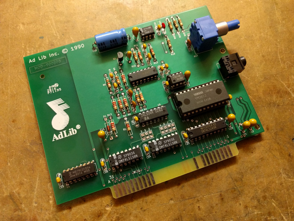
Compare it with the original 1990 version of the AdLib sound card.
I started with Sergey’s OPL2 card and corrected some differences between it and the genuine AdLib card. Since I don’t own a physical card, I found photos on the net of the front and back of the card to use as a reference. To make sure everything matched up exactly, I figured out the design grid of the original and duplicated the traces and component placement as closely as possible. All the library footprints are custom designed to match!
The KiCad design files are available on GitHub. Mouser part numbers are embedded in the KiCad design but they are also included in the table below. The Yamaha OPL2 chipset, the YM3812 and YM3014B pair, can be found at various sources online. They were socketed on many older Sound Blaster cards, so I suspect quite a few were recovered by the scrappers.
| Q | Designator | Description | Mouser Part |
| 1 | J1 | CONN_01X05 | 490-SJ1-3553NG |
| 1 | U6 | YM3812 | |
| 11 | C4,C5,C24,C2,C25,C20,C19,C26,C1,C14,C16 | 0.1uF | 581-AR215C104K4R |
| 1 | D1 | D | 512-1N4148 |
| 1 | Q1 | 2N3904 | 512-2N3904BU |
| 2 | R1,R13 | 8.2K | 291-8.2K-RC |
| 6 | R2,R3,R6,R7,R11,R12 | 2.2K | 291-2.2K-RC |
| 1 | R4 | 12K | 291-12K-RC |
| 4 | R5,R9,R10,R16 | 10K | 291-10K-RC |
| 1 | R8 | 1.5K | 291-1.5K-RC |
| 1 | R14 | POT | 652-91A1A-B24-D15L |
| 3 | R15,R18,R19 | 10 | 291-10-RC |
| 1 | U1 | 74LS109 | 595-SN74LS109AN |
| 2 | U2,U3 | 74LS138 | 595-SN74LS138N |
| 1 | U4 | 74LS245 | 595-SN74LS245N |
| 1 | U5 | 74LS04 | 595-SN74LS04N |
| 1 | U7 | YM3014B | |
| 1 | U8 | RC4136 | 595-RC4136N |
| 1 | U9 | LM386N | 926-LM386N-4/NOPB |
| 1 | C18 | 220uF | 647-TVX1C221MAD |
| 4 | C7,C6,C9,C8 | 4700pF | 581-AR211C472K4R |
| 1 | C12 | 1000pF | 581-AR211C102K4R |
| 1 | C17 | 0.047uF | 581-AR215C473K4R |
| 1 | C13 | 270pF | 594-S271K43SL0N6TK5R |
| 6 | C23,C21,C22,C11,C3,C15 | 10uF | 581-TAP106M025CRW |
| 1 | C10 | 4.7uF | 581-TAP475K016SCS |
| 1 | MNT1 | CONN_01X01 | 534-9202 |
To install the card in a computer, you’ll need to get a Keystone 9202 bracket. The KiCad layout includes a drawing showing where the holes need to be punched in the bracket. I recommend using a hand-held sheet metal punch with a 7mm or 9/32 die. You could also drill it but the punch makes a much cleaner hole.
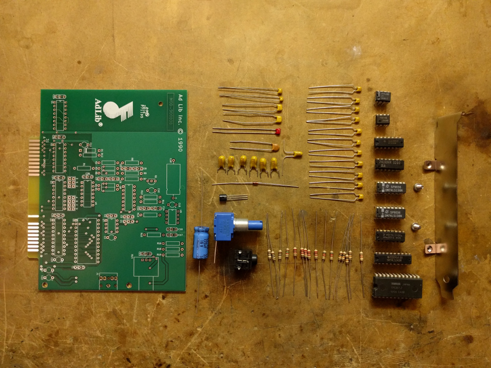
Here’s a bonus photo showing all the parts laid out before soldering. The components were chosen to match the colors on the original card.
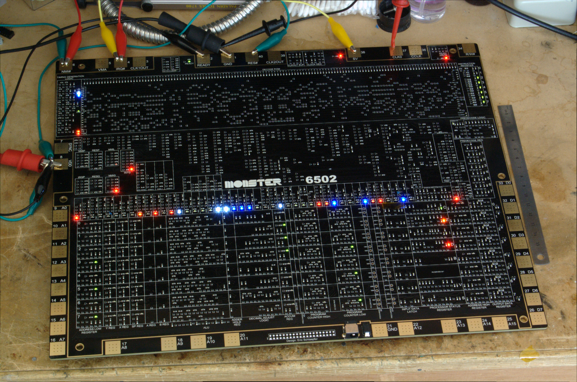
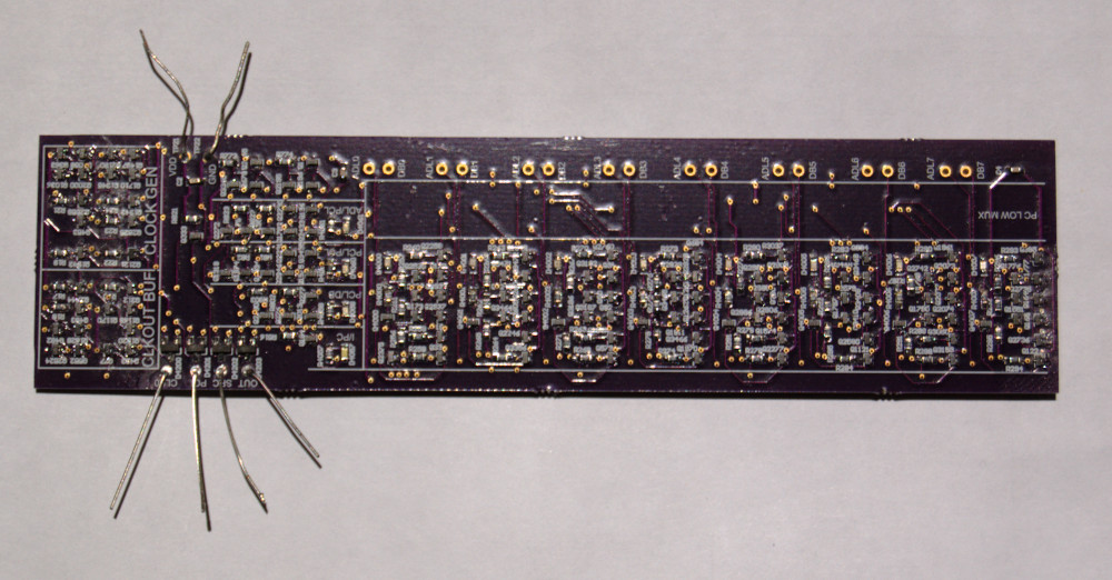
I brought up an additional MOnSter6502 board today. At first it failed my basic validation routines, tripping up on the LDA nn,Y instruction ($B9).
The bus diagnostic output showed that LDA nn,Y was trying to read nn+Y+1 instead of nn+Y (in my test, it accessed $0211 instead of $0210). The LEDs showed that the Y register contained the expected value, so I thought the ALU carry in signal may have been loading a ‘1’ instead of a ‘0’, thus causing the incremented value. I scoped it out and it was fine.
Then I noticed that LDA nn,X worked fine which is totally weird because those instructions are just about identical! So I physically inspected the Y register and saw this tomfoolery:
Those transistors are in bit zero of the Y register. The one on the left prevents anything but a ‘1’ from being in the LSB. The one on the right was supposed to drive the LED on so that I could tell the bit was stuck, but it decided to cover for its dead buddy. I don’t even know how this happened. It could have been shipping damage, or maybe I fat fingered a screwdriver.
After fixing it, the board worked fine. Two dead transistors and a lying LED. Gotta love transistor level debugging.
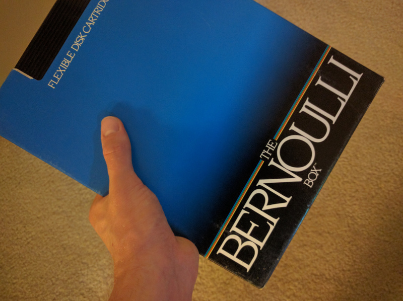
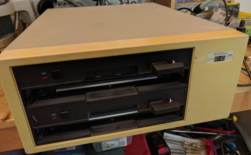
I’ve got an old Bernoulli Box (Model A210H). In the early ’80s, it was a popular way to store 10 megabytes of data in a removable cartridge format. This was also a very common IBM PC hard drive capacity back in those days, so it was great for backups. The cartridge is quite large, and comes in a protective cardboard box:
It’s been 20 years since I last turned it on. After plugging it in and flipping the switch, I smelled smoke so I quickly shut it off. I opened it up (6 screws) and removed a drive (4 screws) and pulled the controller card off of it (4 more screws). Then I noticed a blown tantalum capacitor, so I replaced it. Then I put it all back together again and powered it up with a bench supply (tantalum capacitors nearly always fail in a short circuit which makes things a little too exciting, so at least a bench supply lets me limit the current). More smoke, and another blown tantalum capacitor. I fixed it and put it back together, and powered it up with the regular power supply.
Closing the drive door made the motor spin up very sluggishly, so I checked and noticed the supply voltages were low. So I took apart the power supply and noticed a voltage adjustment potentiometer, so I set it back to the correct voltages and put everything back together. Now the motors seemed to run OK.
I tried putting in a disk and closing the door, but the drive made horrible noises. The LED on the drive blinked and the drive spun down, essentially rejecting the disk. I figured out how to open the protective window on the disk cartridge, and noticed that there were bits of sticky crap on the disk, mostly near the hub in the center. Taking apart the drive, I noticed a rubber ring that is supposed to push down on the disk in order to create some friction to spin it up. The rubber had decomposed into sticky stuff that was getting everywhere.
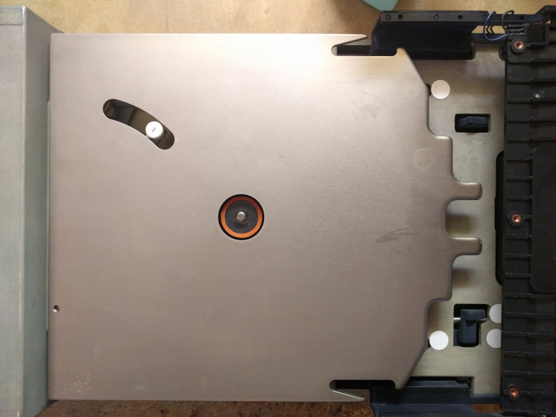
Bernoulli drives work on the Bernoulli principle. The disk itself is basically a floppy disk and is made from thin flexible plastic. There is a metal plate (the Bernoulli plate) that the disk spins up against. As it spins, the air in between the disk and the plate also spins and flies out due to centrifugal force. This creates a vacuum that pulls the disk very close to the plate, stiffening it so much that it acts like a hard disk platter. The drive head floats on an air cushion above the disk surface just like in a hard drive.
Unlike in a hard drive, if any dust particles get pulled into the gap, then the disk drops away from the head and nothing is damaged. The metal plate and the head both need to be very, very clean for the drive to work correctly. They are actually mounted upside down so that dust will fall away and not settle. A large fan on the back of the drive (with an attached air filter) provides positive air pressure in the case to help keep dust out. Before it enters the gap between the plate and the disk, the air is filtered a second time by a very small filter located behind the drive head.
In my drive, the head was filthy, the Bernoulli plate had some dust on it, and had a little oxidation on the back. I removed the oxidation with a file, with the idea that any patches of oxidation could produce problematic dust particles. I cleaned the working surface of the plate and the drive head with special no-lint wipes and 91% isopropyl alcohol. It’s very important not to disturb or distort the working surface, otherwise the disks will not spin right and could be damaged.
I also fabricated a replacement rubber ring and glued it onto the top of the drive spindle. In the photo below you can see the spindle with the new rubber ring. The drive head is the white thing running in the slot on the upper left. The cartridge enters from the right, and you can see some angular protrusions on the plate that open the cartridge and slide back the protective cover.
Fortunately I still had the controller card and the cable, but I had no driver software. I managed to find the DOS driver on some random website, and it actually matched up and worked! I tried it with a different disk and I was able to read back data. A few data errors occurred, but they were mostly soft errors that a couple of retries could fix. I was also able to clean up the original disk using more wipes and isopropyl alcohol. It worked fine although it had some bad sectors.
Where we left off, the MOnSter 6502 had successfully ran a basic validation suite that validated a subset of the instructions but checked every bus cycle for accuracy. Shortly afterwards I was able to get it to run the full validation suite.
BASIC ran just fine after that. It was quite slow with a 6KHz clock but it was enough to run some simple BASIC programs. Typing was difficult because my validation computer uses an Atari POKEY chip to scan the keyboard, and it latches keystrokes very slowly because of the slow bus clock.
I’ve been experimenting with increasing the maximum clock frequency. It helped to reduce the bus capacitance that I added, but if I went too low, it cut into the minimum operating frequency. With less bus capacitance I was able to get the clock up to about 60KHz, and BASIC is quite usable at this speed.
There is an issue I’ve been running into that has to do with the active bus pullups. The pullups are switched on by CCLK (first clock phase), and the pulldowns are normally changed on the CP1 edge (second clock phase). However this is done using a dynamic latch, so if the clock slows down too much, the latch will change state, causing both pullup and pulldown to be turned on at the same time. Here’s an example circuit:
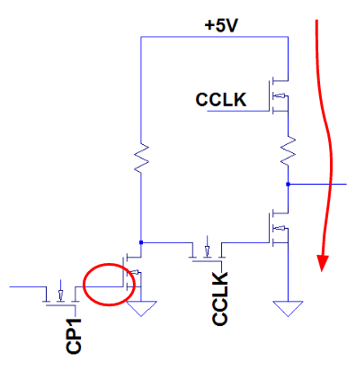
The circled node is the storage node of the dynamic latch. If CP1 is off for too long, then this node can discharge, going from a ‘1’ to a ‘0’. When that happens, the output goes high and drives a ‘1’ into the pulldown transistor when CCLK goes high. CCLK turns on the pullup at the same time. As you can see in the diagram, I’ve added a small resistor in between both transistors to limit the current.
This resistor, although it protects the transistors, also limits the maximum clock speed by limiting how fast the bus capacitance can charge up.
I’ll be experimenting with some alternative ways of protecting the transistors without slowing down the bus too much.
Wow, Maker Faire was totally nuts! Lots of people came by to check out the MOnSter 6502 and I had some interesting conversations with people. After taking a few days to recover, I dug back into the bringup and validation process.
The MOnSter 6502 now passes my basic validation test suite. I discovered two problems.
It was not booting consistently, and kept getting stuck in a bad state where the ‘1’ bit would run off the end of the instruction sequencer, or it would get stuck in a loop running the same (wrong) instruction over and over again. The RESG latch also was stuck on.
When RESET goes low, it turns on RESG. This forces the BRK instruction (which is meant to trigger a software interrupt) into the predecode IR (instruction register) by deasserting D1x1, sets the vector address to the reset vector (instead of the IRQ vector, as BRK normally does), and prevents BRK from writing to the stack so it can’t push the program counter and status bits. When BRK is done, it clears the RESG latch. This is a very clever hack that the original designers used so they could avoid having to run a reset line all over the chip.
Oddly, even when RESG was set (I could tell by a convenient LED), the contents of the IR were not all ‘0’ (again, according to convenient LEDs). Turns out the quad FET array devices used in the IR had some leads that were not soldered down correctly. Fixing that solved the problem.
After trying to run the validation suite again, it started failing the cycle-by-cycle validation on the first time an actual BRK instruction was supposed to be executed. BRK saves the least significant byte of the program counter the most significant byte, and finally the contents of the status register to the stack (with the B bit set so your interrupt service routine can tell the difference between BRK and a hardware IRQ). In this case, it was writing the most significant byte and the status register to the wrong locations in memory.
So I hard-wired the PHA (PusH Accumulator) instruction onto the data bus so I could observe a very simple instruction write to the stack. The value was written correctly, but instead of decrementing the stack pointer by 1, it subtracted 18! PHA decrements the SP by loading it onto the ADL bus and setting the ALU to add with the B input hold register connected to ADL and the A input hold register connected to the special bus. The idea is that by adding $FF you decrease the value by one. This only works if nothing else is driving the special bus except for the precharge pullup MOSFETs. It’s another clever hack from the original 6502 designers. In my case, instead of seeing $FF, the ALU was latching $EE! I tried adding a small amount of capacitance from special bus lines 0 and 4 to ground to keep the voltage up from the precharge cycle, and PHA then worked correctly. I ended up adding capacitors to all the bus lines just in case.
After those fixes my basic validation test suite passed without any further issues.
The next step is to run a more complete set of validation tests, and then BASIC!
So, I made a thing. A really big thing. Really big and really crazy.
You might have seen my discrete 555 and 741 IC electronics kits. Well, a while back I had this idea about creating a discrete version of a microprocessor, but it just sounded too difficult, time consuming, or impractical. And part of me didn’t want to do it, because it just sounds so tedious to design–at every stage, I was secretly hoping to find a show-stopping problem. But part of me was really interested to see if it could be done.
At dinner, Windell and I went through a thought experiment to see if it would even be possible. We weren’t sure how many transistors were in a 6502 (more than 1,000 but less than 10,000). If four surface mount transistors can fit in a square centimeter, then the board would need to be about 1,000 square centimeters, or about 32cm (13in) on a side, which is not as huge as we originally thought. Darn it, time to investigate further!
The hard work of reverse engineering the actual 6502 has already been done by the folks at Visual6502.org. I was able to extract the netlist from their Javascript simulation, which contains a list of all the transistors and every single wire connecting them together.
The 6502 uses dynamic NMOS logic, so it has a large number of “transmission gate” transistors that are used to switch currents. For various technical reasons, only a 4-terminal MOSFET can make an effective NMOS transmission gate. Those are really hard to find (nearly all MOSFETs are 3-terminal devices), but I found one–it’s an array of 4 MOSFETs on a single chip with a separate substrate pin.
I ran simulations using the transistors I found, and noticed that basic combinational logic and latches worked. I ordered parts and prototyped a few circuits. They worked perfectly.
I designed and ordered an OSH Park circuit board with just 8 bits of the program counter register. I thought to myself that there was no way such a complex circuit could work, especially with the ripple carry propagation. Well, it worked.
It was time to bite the bullet. I wrote a Python program that turned the Visual6502 netlist into a 3,510 line spreadsheet, and I began entering (on July 3, 2015) the transistors one by one into the schematic, highlighting each transistor as I finished it. Along the way, I noticed that the Visual6502 netlist had three extra transistors, T1088, T1023, and T3037.
![]()
(An example of an extra transistor)
When I was done with all 61 pages, I wrote another Python program to compare my schematic against the original netlist and corrected a few mistakes. Then I added 167 colorful LEDs to various control lines and data bits, and a few protection components.
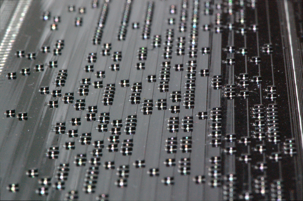
The layout came next. In the layout software, I placed 4,304 parts by hand and wired them up manually (no autorouter) over the course of several months, finishing the last transistor on Dec 1, 2015.
And last Thursday, the first boards came in. They are beautiful!
We’ll be bringing it to Maker Faire, so I have a week to work on bringup testing. Wish me luck!
You can find more details on the main project site, monster6502.com.
A customer recently asked us some questions about the Three Fives discrete 555 timer kit. One in particular really got my attention.
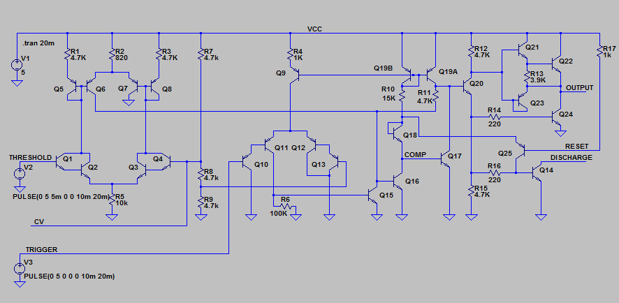
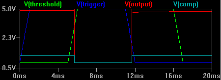
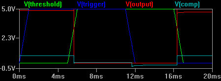
What is the difference between the National Semiconductor LM555 and the Signetics NE555 timer ICs? Well, the Signetics part certainly came first and the National part was a second source, but the customer noted that The 555 Timer Applications Sourcebook, on page 5-31, states
…Table S-2 points out that the threshold overrides the trigger for the type LM555H (National), but the threshold is overridden by the trigger for the type NE555V (Signetics).
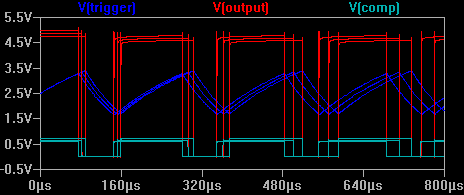
Let’s compare the two. First, here’s the NE555 schematic (click for larger versions).
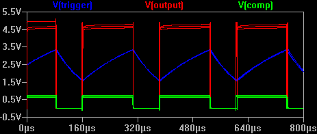
And here’s the LM555 schematic. I’ve kept the component numbering consistent with the NE555 datasheet rather than National’s datasheet to make comparisons easy.
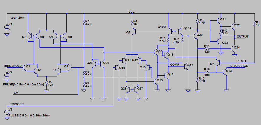
The LM555 makes three minor changes to the timer design:
The most interesting changes are the first two. How do these changes reverse the priority of the two comparator inputs?
The original NE555 gives priority to the trigger signal because transistor Q15 can always overpower the current coming from Q19A and Q6.
Inspired by commenter Katemonster, I’ve put together a short clip with a couple of CRTs from my collection, demonstrating various types of phosphors. There are charts out there that talk about persistence using vague terms like “medium” (compared to what?), so it’s nice to see a real video showing what such a CRT actually looks like.
For the video I’ve used my “orbiter” demo that uses Newton’s law of gravity and Newton’s 2nd law of motion (F=MA) to generate simulated planets that orbit around a sun. It’s a nice way to demonstrate persistence (the way the phosphor fades as the electron beam moves away).
P1 Phosphor
This is the basic green phosphor. At 525nm primary color wavelength, it looks slightly more blue than common super-bright green LEDs. The chart linked above lists the persistence time as 20ms which seems reasonable. The formulation for this phosphor varies between manufacturers so some tubes might be slower than others. It’s very common in early oscilloscopes and oscillographs, and apparently some radar systems as well.
P2 Phosphor
The P2 phosphor color has even more blue in it than the P1–it’s very close to “stoplight green”. The persistence is much longer as you can see in the video (30 seconds or more, depending on the ambient light levels). The charts and reference documents I have list the primary applications as oscillography and radar.
P7 Phosphor
P7 is a very interesting phosphor. It is a cascade phosphor, meaning that it has two layers of material. The electron beam strikes the first (outer) layer which emits a bright blue light with some light near ultraviolet. This high energy light excites the second layer (inner, in contact with the glass) which is a much slower material that emits a yellowish-green light with a very long persistence (around a minute). In the video I move the “orbit” trace off to the side so you can see that original afterimage persists.
It was used mostly for radar and sometimes in oscilloscopes to capture one-time events before storage tubes were invented.
So why use a cascade phosphor? One source states that it was originally designed to be used in intensity-modulated displays (varying brightness levels), but it turns out it also helped prevent radar jamming. Since the jamming signal was not synced to the radar pulses, a long persistence phosphor could average out the jamming signal and allow the operator to see the true signal as viewed on an A-scope (time-based pulse waveform monitor). [Cathode Ray Tube Displays, MIT Radiation Laboratory Series, pg. 626]
P12 Phosphor
This one is my favorite. It’s an orange medium-persistence (a few seconds) phosphor that was apparently used for radar indicators. I don’t know of any that were used in oscilloscopes.
P31 Phosphor
The P31 phosphor was invented as an improved P1 phosphor. It’s much brighter (P1 is 32% as bright) and has short persistence (<1ms). The color has a bit more blue in it–in fact, very close to the P2 phosphor’s color. I would say most analog oscilloscopes from the 70s to today use CRTs with the P31 phosphor.
In many cases these CRTs would be installed behind a colored piece of plastic acting as a color filter. For example, P7 CRTs were often installed with an orange plastic filter in front to make the blue/white phosphor look more similar to the secondary yellow phosphor. P31 CRTs usually have a blue or green plastic filter.
For further reading:
Take a look at my crt-driver GitHub repository. I tidied things up a bit and more importantly, released the Altium project files, schematics, boards, and even the output job file. It’s all licensed under the Creative Commons Attribution-ShareAlike 3.0 license. Read the Creative Commons page for the full terms, but basically you can share or adapt any of it as long as you give me credit (a link to this blog would be appreciated) and make sure that you keep the same license so that others can do the same.
If you don’t have Altium (expensive, closed source), you can at least open and edit the schematics with CircuitMaker (free, closed source, limited). Sadly, CircuitMaker will not let you edit the Altium PCB layout.